Samsung S3 Circuit Board Diagram
Schematic i9300 gt galaxy s4 pcb s5 samsung i9500 Galaxy s ii teardown – splitting 8.9 mm of the latest samsung Gt-i9300 galaxy s3 pcb schematic
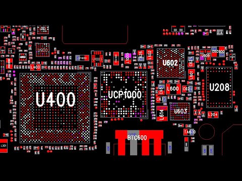
Samsung Galaxy S3 i9300 Schematics
Galaxy s schematics Samsung galaxy teardown circuit technologies splitting mm ii latest global main board Galaxy schematics samsung s3
Samsung galaxy s3 i9300 schematics
I9300 schematics tháng sáu pham commentsMotherboard pcb 4g mainboard android broadcom 3g 3/1/11 ~ mobile phone repair guides.
.


Samsung Galaxy S3 i9300 Schematics
GT-I9300 Galaxy S3 pcb schematic - YouTube

3/1/11 ~ Mobile Phone Repair Guides

Galaxy S II Teardown – Splitting 8.9 mm of the latest Samsung
